Our research focuses on magnetic and photonic materials and devices to gain a better understanding of light-matter, spin-light, voltage-spin interactions. We use this understanding for developing integrated spin-wave and photonic devices for computation and telecommunication applications. We design thin film functional oxides from first principles, experimentally grow, characterize, and then optimize these materials. Once the important properties such as magnetic moment, coercivity, magneto-optical Faraday rotation, optical absorption and Gilbert damping of the thin films are bulk-like or acceptable for our desired applications, we use micro- and nanopatterning techniques to fabricate spin-wave devices. We design interferometric, current or voltage-controlled spin wave devices. The spin-wave device designs are validated and refined using open-source OOMMF micromagnetic simulation software which calculates the time evolution of spin states over finite mesh based on Landau-Lifschitz-Gilbert equation. After the devices are fabricated, their spin-wave processing, magnetic and photonic properties are characterized.
We focus our research on three themes: discovering and experimentally growing high-quality functional oxide thin films, applying these films to spin-wave devices for telecommunication and spin-wave logic applications, and applying these films to photonic sensing applications including magneto-optical surface-enhanced Raman spectroscopy.
Research Theme 1: Design, Growth, Characterization, and Optimization of Functional Oxide Thin Films

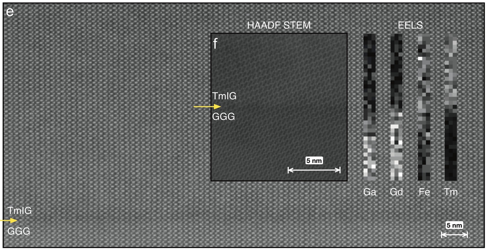
Figure 1. High-resolution transmission electron micrograph of TmIG/GGG (111) films grown using PLD [8].
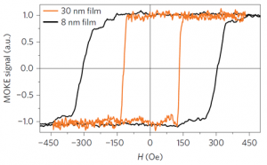
Our recent publications on this subject include demonstration of ultra-low damping garnet thin films with in-plane easy axis (YIG, Y3Fe5O12) [1-7], perpendicular magnetic anisotropy (TmIG, Tm3Fe5O12) [8,9], growth of high-quality thin film magneto-optical oxides on silicon-based substrates [10-13] and on GGG [14].
Research Theme 2: Fabrication and Testing of Spin-wave Logic and Memory Devices
As Moore’s Law can no longer be sustained due to transistor leakage and power dissipation, microprocessor clock rates can no longer be increased beyond 5 GHz. In addition, growing demand for wider bandwidth telecommunications require researchers and engineers to design chips that can consume much less power than state-of-the-art Si CMOS transceivers and microprocessors. An emerging class of solutions for these issues is using spin waves for data processing and storage at room temperature on integrated monolithic chips. Magnetic insulators such as YIG and TmIG with low Gilbert damping allow researchers to eliminate most of Ohmic dissipations with magnon wave propagation and achieve operation frequencies from 1 GHz to 7 THz (1st magnonic Brillouin Zone in YIG), contactless wiring with radiofrequency antennas, wave-based nonlinear processing (i.e. interferometric design of logic gates), nonvolatile computation elements (hard disk drives are converging with RAM’s), less strict fabrication constraints than in Si CMOS (multiple microns vs. sub-10 nm) and simplify the chip layout design in integrated circuits using interferometric spin-wave logic gates instead of several tens of transistors.
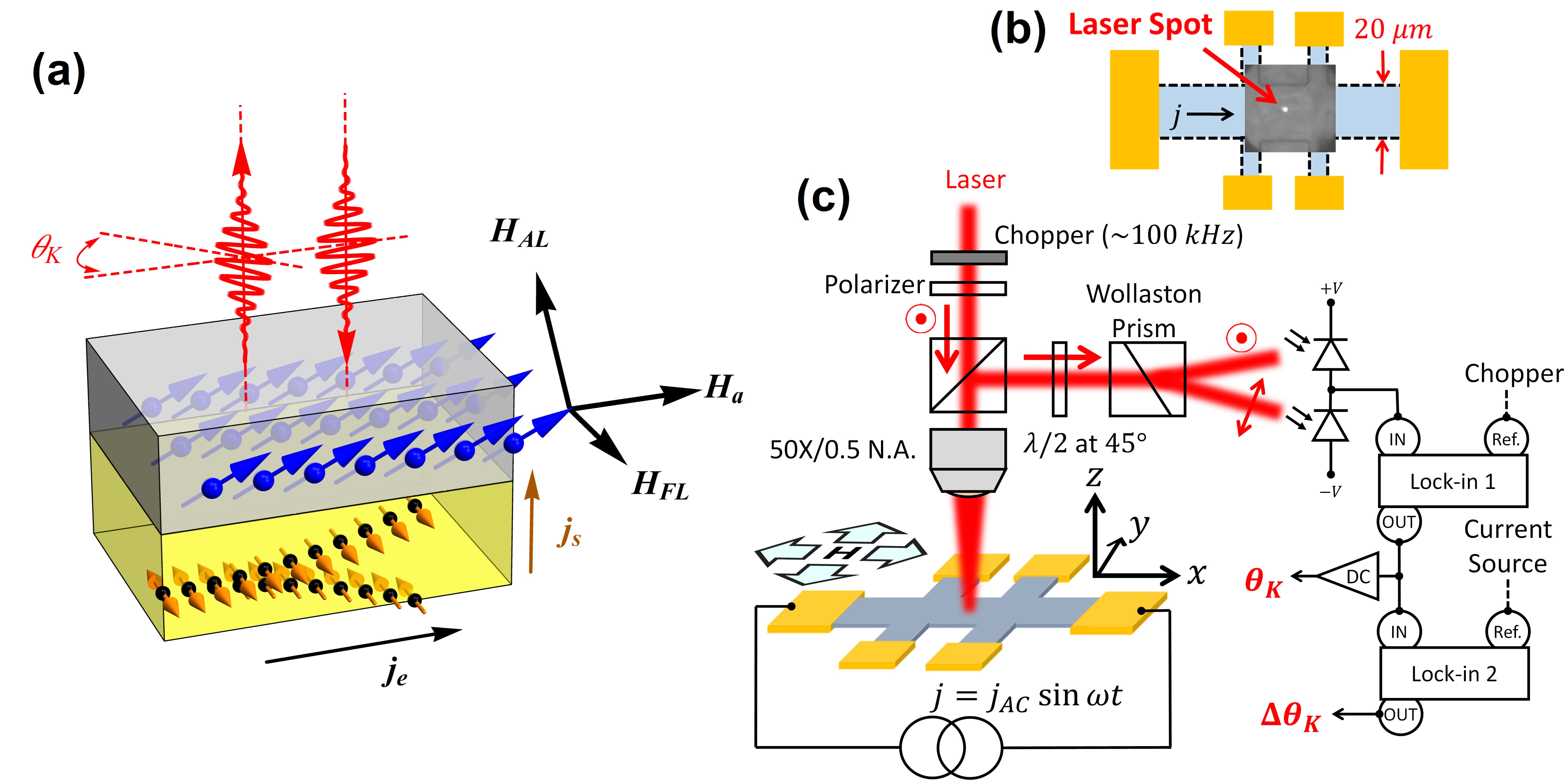
In this research theme, we focus on both fundamental investigations as well as applications of spin wave devices. To advance our fundamental understanding of spin wave propagation in magnetic thin films, we investigate efficient means of injecting spin currents into magnetic insulators through photonic excitations (femtosecond laser pulse, x-ray), thermal (spin Seebeck effect), current-induced (Oersted field, spin-orbit torque, spin-transfer torque) and proximity-induced effects (direct magnetostatic proximity, Rashba effect, voltage-controlled anisotropy) and measure the spin-wave transmission behavior of the devices.Our recent publications on this subject include demonstration of proximity-induced magnetism in topological insulators [15,16], current-controlled switching in a magnetic insulator (TmIG, Tm3Fe5O12) [9], spin Seebeck effect [3,6,17], spin-transfer torque studies and measurement of the spin chemical potential [18].
Research Theme 3: Applications of Inverse Design Methods to Photonic and Magneto-optical Materials in Surface-enhanced Raman Spectroscopy
Raman scattering is an inelastic light-matter interaction process in which a coherent light incident on a molecule is absorbed and then reemitted at a slightly different wavelength due to the vibrational, rotational and other molecule-specific energy modes. These reemitted wavelengths are unique characteristic signatures of each molecule and these wavelength spectra are called Raman spectra. Since one observes molecule-specific responses in Raman spectra, Raman spectroscopy has been developed to detect the existence and concentration of molecules. Using plasmonics, Raman scattering signal intensity can be enhanced for individual molecules and single molecule detection has been demonstrated using plasmonic substrates. As a result, surface enhanced Raman spectroscopy has started becoming a major method for sensing and diagnosis.
The ability to control optical, magnetic, and magneto-optical properties of functional oxides using magnetic field and voltage enables us to further investigate the magnetic field and voltage dependence of Raman scattering of photonic patterned substrates. In this study, we investigate the effect of magnetic field on the plasmon and Raman spectra of photonic substrates with and without analyte molecules.
References
- M. C. Onbasli, A. Kehlberger, D. H. Kim, G. Jakob, M. Kläui, A. V. Chumak, B. Hillebrands, C. A. Ross, “Pulsed laser deposition of epitaxial yttrium iron garnet films with low Gilbert damping and bulk-like magnetization”, APL Materials 2, 106102 (2014).
- Montazeri, P. Upadhyaya, M. C. Onbasli, G. Yu, K. L. Wong, M. Lang, Y. Fan, P. K. Amiri, R. N. Schwartz, C. A. Ross, K. L. Wang, “Magneto-optical investigation of spin–orbit torques in metallic and insulating magnetic heterostructures”,Nature Communications 6:8958 doi: 10.1038/ncomms9958 (2015).
- A. Kehlberger, U. Ritzmann, D. Hinzke, E.-J. Guo, J. Cramer, G. Jakob, M. C. Onbasli, D. H. Kim, C. A. Ross, M. B. Jungfleisch, B. Hillebrands, U. Nowak, and M. Kläui, “Length Scale of the Spin Seebeck Effect”, Physical Review Letters 115, 096602 (2015).
- A. Kehlberger, K. Richter, M. C. Onbasli, G. Jakob, D. H. Kim, T. Goto, C. A. Ross, G. Götz, G. Reiss, T. Kuschel, M. Kläui, “Enhanced magnetooptic Kerr effect and magnetic properties of epitaxial Ce1Y2Fe5O12 thin films”, Physical Review Applied 4, 014008 (2015).
- M. B. Jungfleisch, A. V. Chumak, A. Kehlberger, V. Lauer, D. H. Kim, M. C. Onbasli, C. A. Ross, M. Kläui, and B. Hillebrands, “Thickness and power dependence of the spin-pumping effect in Y3Fe5O12/Pt heterostructures measured by the inverse spin Hall effect”, Physical Review B 91, 134407 (2015).
- A. Kehlberger, G. Jakob, M. C. Onbasli, D. H. Kim, C. A. Ross, M. Kläui, “Investigation of the magnetic properties of insulating thin films using the longitudinal spin Seebeck effect”, J. Appl. Phys. 115, 17C731 (2014).
- Bi, J. Hu, P. Jiang, H. S. Kim, D. H. Kim, M. C. Onbasli, G. F Dionne, C. A Ross, “Magneto-Optical Thin Films for On-Chip Monolithic Integration of Non-Reciprocal Photonic Devices”, Materials 6, 5094 (2014).
- A. Quindeau, C. O. Avci, W. Liu, C. Sun, M. Mann, A. S. Tang, M. C. Onbasli, D. Bono, P. M. Voyles, Y. Xu, J. Robinson, G. S. D. Beach, C. A. Ross, “Tm3Fe5O12 Ultrathin Films with Perpendicular Magnetic Anisotropy for Spintronic Applications,” Advanced Electronic Materials 3, 1, (2017).
- C. O. Avci, A. Quindeau, C.-F. Pai, M. Mann, L. Caretta, A. Tang, M. C. Onbasli, C. Ross, Geoffrey S. D. Beach, “Tm3Fe5O12 Ultrathin Films with Perpendicular Magnetic Anisotropy for Spintronic Applications, “Current-Induced Switching in a Magnetic Insulator”, Nature Materials 16, 309 (2017).
- Taichi Goto, C. Onbasli, Caroline A. Ross, “Magneto-optical properties of cerium substituted yttrium iron garnet films with reduced thermal budget for monolithic photonic integrated circuits”, Optics Express, 20, 28517 (2012).
- M. C. Onbasli, T. Goto, X. Sun, N. Huynh, C. A. Ross, “Integration of bulk-quality thin film magneto-optical cerium-doped yttrium iron garnet on silicon nitride photonic substrates”, Optics Express 22, 25183 (2014).
- T. Goto, M. C. Onbasli, D. H. Kim, V. Singh, M. Inoue, L. C. Kimerling, C. A. Ross, “A nonreciprocal racetrack resonator based on vacuum-annealed magnetooptical cerium-substituted yttrium iron garnet”, Optics Express 22, 19047 (2014).
- Taichi Goto, M. C. Onbasli, Caroline A. Ross, “Magneto-optical properties of cerium substituted yttrium iron garnet films with reduced thermal budget for monolithic photonic integrated circuits”, Optics Express, 20, 28517 (2012).
- C. Onbasli, L. Beran, M. Zahradník, M. Kučera, R. Antoš, J. Mistrík, G. F. Dionne, M. Veis, C. A. Ross, “Optical and magneto-optical behavior of Cerium Yttrium Iron Garnet thin films at wavelengths of 200 – 1770 nm”, Scientific Reports 6, 23640 (2016).
- M. Lang, M. Montazeri, M. C. Onbasli, X. Kou, Y. Fan, P. Upadhyaya, K. Yao, F. Liu, Y. Jiang, W. Jiang, K. L Wong, G. Yu, J. Tang, T. Nie, L. He, R. N Schwartz, Y. Wang, C. A. Ross, K. L. Wang, “Proximity Induced High Temperature Magnetic Order in Topological Insulator-Ferrimagnetic Insulator Heterostructure”, Nano Letters 14, 3459 (2014).
- W. Liu, L. He, Y. Xu, K. Murata, M. C. Onbasli, M. Lang, N. Maltby, S. Li, X. Wang, C. A. Ross, P. Bencok, G. van der Laan, R. Zhang, Rong; K. Wang, “Enhancing Magnetic Ordering in Cr-doped Bi2Se3 using High-TC Ferrimagnetic Insulator”, Nano Letters 15, 764 (2015).
- A. Kehlberger, G. Jakob, M. C. Onbasli, D. H. Kim, C. A. Ross, M. Kläui, “Investigation of the magnetic properties of insulating thin films using the longitudinal spin Seebeck effect”, J. Appl. Phys. 115, 17C731 (2014).
- C. Du et al., “Control and local measurement of the spin chemical potential in a magnetic insulator” (in press) Science (2017). (arXiv preprint arXiv:1611.07408).

